About
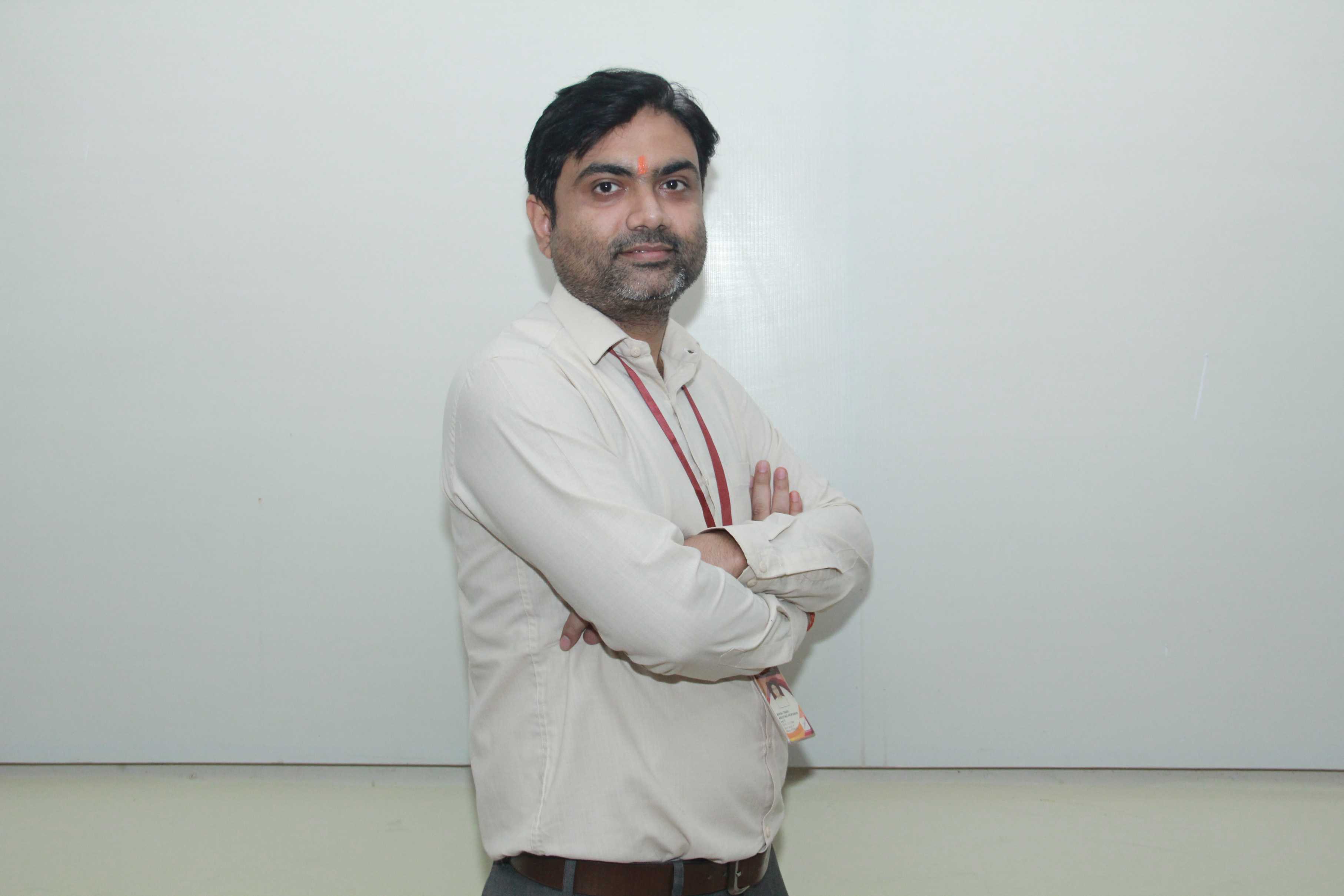
| Educational Qualication | Ph.D (pursuing), M.E., B.E. |
|---|---|
| Area of Interest | Analog and Digital VLSI, VLSI Testing, Nanomaterial Modeling |
Journals Publications
- Title: Theoretical analysis and design of microphotodiodes materials for artificial retina implant Project Cost: 5 Lakhs Funded by: TEQIP-III Status: Completed
Patent Published
- 1. Application Number: 2021105083 Australian Patent, Title of Invention: “Quantum Computing Machine Learning Module and System”, Date of Filing: 07/08/2021, Publication Date: 07/08/2021, Status: Granted.
- 2. Application Number: 202011009101 Title of Invention: “ITMD-DEVICE: Intelligent Technology To Maximize The Display Area Of A Mobile Device”, Date of Filing: 03/03/2020, Publication Date (U/S 11a):20/03/2020, Application Status: Published.
- 3. Application Number: 202041006276 Title of Invention: “IPCPC-VLSI-Circuits: Intelligent Process Of Computing Dual-Conductor Parasitic Advanced Capacitances For VLSI Circuits”, Date of Filing: 13/02/2020, Publication Date (U/S 11a):21/02/2020, Application Status: Published.
Book Chapter
- M. L. Verma and Ashish Tiwari, “Suitable nanomaterials for Retinal implant technique and future trends”, in the chapter for book titled Advanced Materials and Nanosystems: Theory and Experiment, Bentham Science Publishers. (Article under press)
Journals Publications
- Mohan L. Verma, Ashish Tiwari, Theoretical investigation on structural transformation of TiN to HfN monolayer: A first principles study, in, “Chemical Physics Letters”, Volume 781, 2021, ISSN: 0009-2614. (Elsevier) (IF:2.328)
- Ashish Tiwari, R.H.Talwekar, Mohan L. Verma “First-Principles Study on the Structural, Electronic, Optical, Mechanical, and Adsorption Properties of Cubical Transition Metal Nitrides MN (M = Ti, Zr and Hf)”, in, “Journal of Electronic Materials”, Volume 50 Issue 6, page 3312–3325, 2021, ISSN: 0361-5235. (Springer Nature) (IF:1.77)
- Ashish Tiwari and R.H.Talwekar, “Analysis and mathematical modeling of charge injection effect for efficient performance of CMOS imagers and CDS circuit”, in, “IET Circuits, Devices & Systems”, Volume 14 Issue 7, page 1038-1048, October 2020, ISSN: 1751-858X. (The Institution of Engineering and Technology)(IF:1.29)
- Ashish Tiwari and R.H.Talwekar, “Journey of Visual Prosthesis with progressive development of electrode design techniques and experience with CMOS image sensors: A Review”, in, “IETE Journal of Research”, Volume 65 Issue 2, page 172–200, 2019, ISSN: 0377-2063. (Taylor & Francis)(IF: 1.12)
- Ashish Tiwari and R.H.Talwekar, “Optical property analysis of transition and alkaline metal doped MoS2 bulk layers for photo-sensor applications” in, “Materials today proceedings”, Elsevier, 2021.
- Ashish Tiwari and R.H.Talwekar, “Review On Progressive Development of Cmos Imagers for Visual Prosthesis and New Aspects” in, “Journal of Advanced Research in Dynamical and Control Systems”, Volume 9. Sp– 14, page 1334-1348, 2017, ISSN: 1943-023X.
- Ashish Tiwari and Renu Prabha Sahu, “Design and Analysis of Low Power PLL for Digital Applications”, Advances in Intelligent systems and computing series, ISSN: 2194-5357.
- Ashish Tiwari and Renu Prabha Sahu, “A Review on Design and Analysis of Low Power PLL for Digital Applications”, International Journal for Research in Applied Science and Engineering Technology, Volume 6 Issue, June 2018, ISSN: 2321-5693. (ISI, Academia.edu, Research Bible).
- Ashish Tiwari, Snehlata Raisagar, Kajal Tiwari “Robust Visual Tracking using Sparse Principle Component Analysis and Haar-like Features” published in “International Journal for Scientific Research & Development”, volume 5, issue 9, 2017, page 519-524, ISSN: 2321-0613. (Academia.edu, Google scholar, Isuue).
- Snehlata Raisagar and Ashish Tiwari, “A Survey on Object Tracking in Video” published in “International Journal for Scientific Research & Development”, volume 5 issue 7, page 820-225, 2017, ISSN: 2321-0613. (Academia.edu, Google scholar, Isuue).
- Ashish Tiwari “Testing of Mixed Signal ICs: A Review” published in Global Journal for Research Analysis, Volume 3, Issue 8, August 2014, ISSN: 2277-8160. (UGC, Crossref, Pubmed).
- Ashish Tiwari and Anil Kumar Sahu, “Mixed Signal IC (CP-PLL) Testing scheme using a novel approach” published in “International Journal of Scientific & Engineering Research”, Volume 3 Issue 5, May-2012, ISSN: 2229-5518. (Crossref)
- Ashish Tiwari, Anil Kumar Sahu and Dr. G. R. Sinha, “Design for testability architecture using existing elements of CP-PLL for Digital Testing Applications in VLSI ASIC Design” published in “International journal of VLSI and Signal Processing Applications”, volume 2 issue 1, Feb 2012, (56-64), ISSN: 2231-3133. (Crossref, Harvard library, Google scholar).
- Ashish Tiwari, Anil Kumar Sahu, Dr. G. R. Sinha, and Dr. V.K.Chandra, “A novel approach of stimulus generation and measurement for BIST in CP-PLL testing scheme” published in “International journal of Computer Science and Information Security”, Volume 10 Issue 2, Jan 2012, ISSN: 1947-5500.
Conferences/ Seminars
- Ashish Tiwari and R.H.Talwekar, “Structural and Electronic property analysis of transition and alkaline metal doped MoS2 bulk layers for photo-sensor applications” in, IEEE International Conference on Computing, Communication and Automation, Fri, 17 Dec, 2021 – Sun, 19 Dec, 2021.
- Ashish Tiwari and R. H. Talwekar, “Mathematical modeling of non-linearity due to charge injection effect in CMOS Imagers” at IEEE International conference on Advances in Electrical, Computing, Communications and Sustainable Technologies (ICAECT), 19-20 Feb 2021, SSTC, Bhilai, Chhattisgarh.
- Ashish Tiwari and R.H.Talwekar, “Clocking scheme, Reset noise analysis and reduction technique for CMOS Image Sensors utilized in Subretinal Implant”, 2019 5th IEEE International Conference for Convergence in Technology (I2CT), Pune, India. Mar 29-31, 2019.
- Ashish Tiwari and R. H. Talwekar, "Implementation of a novel 2-stage DFT structure for CMOS pixel sensors utilizing on-chip CP-PLL clock (for retinal implant system)," 2017 IEEE International conference on Microelectronic Devices, Circuits and Systems (ICMDCS), Vellore, India, 2017, pp. 1-6.
- Ashish Tiwari and A. K. Sahu, "An innovative approach of computational fault detection using design for testability of CP-PLL," 2012 IEEE National conference on computing and communication systems, Durgapur, 2012, pp.1-6.
- Ashish Tiwari and Renu Prabha Sahu, “Implementation of five-stage CS-VCO circuit on 250nm CMOS technology in PLL for Low Power Digital Applications,” International Journal of Electrical and Electronics Research, Volume 6 Issue 3, July 2018- September 2018, ISSN: 2347-470X. (ISI, Academia.edu, Research Bible). Other Conference:
- Ashish Tiwari and Chandradatta Verma, “Implementation of an efficient low –area CP-PLL DFT architecture for testing applications “in AICON 19-21 January 2012 organized by Chhatrapati Shivaji Institute of Technology.
- Chandradatta Verma and Ashish Tiwari, “A novel approach to low power Analog to Digital Converter using parallel realization “in AICON 19-21 January 2012 organized by Chhatrapati Shivaji Institute of Technology.
- Ashish Tiwari, Megha Pandey, Umesh P. Akare and Laxman P. Thakare, “Implementation of an efficient multiplier based on Vedic algorithm”, an IETE National conference organized by KITS, Ramtek, Nagpur 2009.
- Ashish Tiwari, Megha Pandey “Implementation of multiplier based on Nikhilam algorithm”, presented a paper in Technologia 2010, organized by “M.P. Christian College of Engineering and Technology”, won second prize for this presentation.
Awards/Recognitions
- Reviewer of IEEE International Conference on Electrical, Computer, Communications and Mechatronics Engineering, 2021, the University of Mauritius.
- Reviewer of 3rd IEEE Bombay Section Signature Conference 2021 by Indian Institute of Information Technology & Management, Gwalior India.
Training Programmes/Workshops Attended
- Six days faculty development programme from 10th December 2021 to 15th December 2021 on “Smart prospective of IoT in different applications”, organized by Shri Shankaracharya Technical Campus, Bhilai under the AICTE-CSVTU TTP (teachers training program) scheme.
- Six days faculty development programme from 26 June 2021 to 1st July 2021 on “Green Technology and Sustainable Engineering”, organized by Bhilai Institute of Technology, Raipur under the AICTE-CSVTU TTP (teachers training program) scheme.
- Five days faculty development programme from 22 June 2020 to 26 June 2020 on “Cutting edge technological development in Information and Communication Engineering”, organized by Bharat Institute of Engineering & Technology, Hyderabad.
- Five days faculty development programme from 11 June 2020 to 26 June 2020 on Scilab organized by Chhattisgarh Swami Vivekanand Technical University with course material provided by Spoken Tutorial Project, IIT Bombay.
- Five days faculty development programme from 29 April 2020 to 02 May 2020 on Scilab organized by Chhattisgarh Swami Vivekanand Technical University with course material provided by Spoken Tutorial Project, IIT Bombay.
- One day workshop on “Motivation and Leadership Skills” s by IIT Hyderabad on 6th august 2016.
- Six days workshop on “Materials Modeling for Device Applications” organized by Shri Shankaracharya Technical Campus-SSGI, Bhilai on 31st August 2019 under TEQIP-III.
- Five days faculty development programme from 02 Jan 2018 to 06 Jan 2018 on “Advancement in power system and power Electronics” organized by Chhatrapati Shivaji Institute of Technology, Durg (C.G.).
- Five days National workshop on “Emerging Technologies in Power Electronic, Electric Drives and Power Systems” organized by Rungta College of Engineering and Technology, Bhilai from 25th Dec 2016 to 29th Dec 2016.
- One day workshop on “Digital Design using Arduino” organized by IIT Hyderabad on 6th august 2016.
- Two days National workshop on “Advancement in Communication Technology and Application” organized by Raipur Institute of Technology, Raipur on 30th and 31st Jan 2016.
- Two week ISTE workshop on Control Systems conducted by Indian Institute of Technology Kharagpur from 2nd December to 12th December 2014.
- National workshop on “CMOS VLSI Design using Tanner Spice”, Organized by CCET, Bhilai on 16th December 2011.
- National workshop on “Intellectual Propriety Rights” Organized by MSME government of INDIA with SSCET, Bhilai, on 6th February 2012.
- Invited Speaker at “International Conference on Vedic Sciences and its Applications (I.C.V.S.A.)” organized by “Chhattisgarh Vigyan Bharti” at Pandit Ravishankarshukla University Raipur on 19-20th November 2010, on the topic of implementation of high efficient multiplier & square architecture.


